The silicon lattice has. Lattice planes are represented by the vector that is normal perpendicular to them these are 3D.
Silicon And Germanium


Monocrystalline Silicon An Overview Sciencedirect Topics
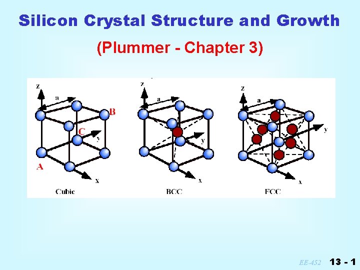
Silicon Crystal Structure And Growth Plummer Chapter 3
Deposition and etch properties are highly dependent upon surface structure and chemistry.
Silicon lattice structure. The geometry of the unit cell is defined as a parallelepiped providing six lattice parameters taken as the lengths of the cell edges a b c and the angles between them α β γ. Silicon and Germanium are examples of covalent crystals. 3C 4H and 6H.
This makes silicon a stable element when compared to Germanium and reduces the chance of leakage current. The tetrahedral form is the basic unit from which a SiO structure is formed even though SiO can exist in a crystalline structure. Groups of equivalent directions or planes are called families.
Solar cells made out of silicon currently provide a combination of high efficiency low cost and long lifetime. Crystal structure Lattice Basis 4. Centered cubic crystal structure found in carbon silicon α-Sn and other covalently bonded materials.
In these solids the atoms are linked to each other by covalent bonds rather than by electrostatic forces or by delocalized valence electrons that work in metals almost like a glue. Lattice Diamond design software offers leading-edge design and implementation tools optimized for cost sensitive low-power Lattice FPGA architectures. This lattice provides an organized structure that makes conversion of light into electricity more efficient.
Table I lists the Miller index notation for cubic crystals. The substructure can be made of wood or stainless steel. Silicon is a hard and brittle crystalline solid with a blue-grey metallic lustre it is a tetravalent metalloid and semiconductor.
The cube side for silicon is 0543 nm. So far we have treated all atoms in the crystal structure as equal and ignored that quartz is a compound made of silicon and oxygen SiO 2. The reason for the amorphous oxide structure is the absence of any crystalline form of SiO whose lattice size closely matches the silicon lattice 175.
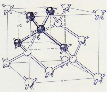
The arrangement of sulfide ions is identical to the arrangement of chloride ions in sodium chloride The radius of a zinc ion is only about 40 of the radius of a sulfide ion so these small Zn 2 ions are located in alternating tetrahedral holes that is in one half of the tetrahedral holes. Different growth planes and orientations have different arrangements of the atoms or lattice. Silicon crystallizes in the same pattern as diamond in a structure which Ashcroft and Mermin call two interpenetrating face-centered cubic primitive latticesThe lines between silicon atoms in the lattice illustration indicate nearest-neighbor bonds.
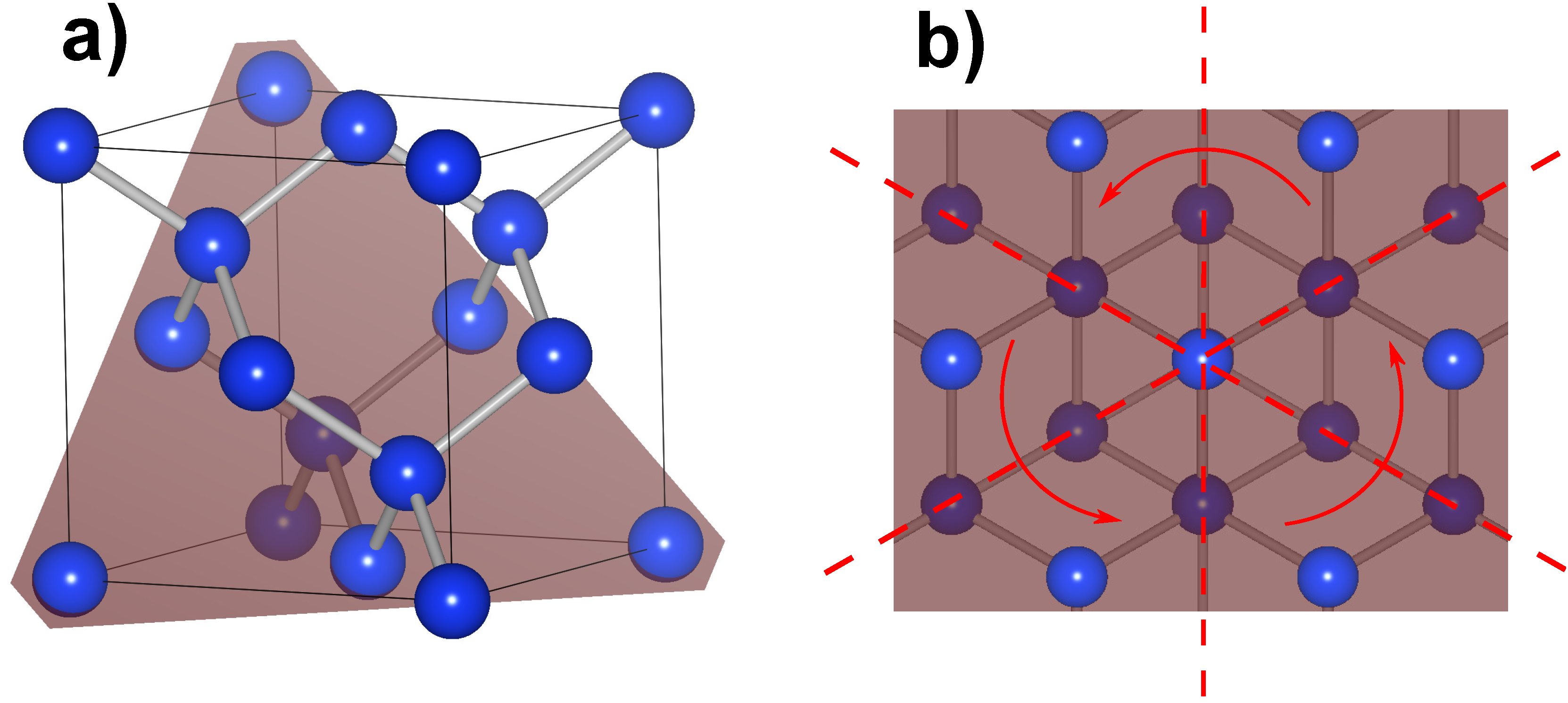
For example in a cubic crystal directions 100 010 and 001 are in the 100 family. In all main polytypes of SiC some atoms have been observed in association both with cubic C with hexagonal H and with rombohedral R lattice sites. This forms a tetrahedrical structure where each atom is surrounded by four equal-distanced neighbours.
A wood lattice substructure is. Crystalline structure of Silicon consists of face centric cubic lattice structure with 34 packing. The underlying structure is fcc with a two-atomic basis.
The chemical symbol for Silicon is Si. The reverse current is in nano-amperes and is very low. Crystal structure is described in terms of the geometry of arrangement of particles in the unit cell.
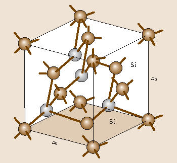
Crystalline silicon cells are made of silicon atoms connected to one another to form a crystal lattice. Silicon possesses a moderate energy band gap of 112eV at 0 K. Conventional unit cell of the diamond structure.
The most classic example of covalent crystal is the diamond that belongs to the fcc cubic crystal system. Diamonds cubic structure is in the Fd 3 m space group space group 227 which follows the face-centered cubic Bravais latticeThe lattice describes the repeat pattern. Carbon silicon and germanium germanium like silicon is also a semiconductor have a unique property in their electron structure -- each has four electrons in its outer orbital.
The videos below include an overview of new features in Diamond along with several key improvements and changes in. Orientations are described using Miller Indices such as 100 111 110 etc. Stereographic projection of silicon crystal.
One of the two atoms is sitting on the lattice point and the other one is shifted by frac14 along each axes. Silicon is a chemical element with atomic number 14 which means there are 14 protons and 14 electrons in the atomic structure. Ee4494 silicon basicsppt revised 09112001 copyright james t yardley 2001 Page 16 Surface properties of silicon.
We used neutron Pendellösung interferometry to make precision measurements of the 220 and 400 neutron-silicon structure factors and achieved a factor-of-four improvement in the 111 structure. The atomic structure of graphene can be observed directly by transmission electron microscopy TEM Fig. The growth plane of the crystalline silicon.
The unit cell is defined as the smallest repeating unit having the full symmetry of the crystal structure. If a crystal is made up of covalently bonded atoms it can be described as a covalent lattice or infinite covalent lattice. Silicon a very common element is used as the raw material of semiconductors because of its stable structure.
However about 95 of all publications deal with three main polytypes. Diamond Cubic Crystal Structure. The solar tiles are screwed directly into the sun-roof structure.
2b which is particularly useful for the evaluation of the different structures such as vacancy defects bond rotations dislocation edges grain boundaries layer stacking and other features Scanning tunnelling microscopy STM can provide information about the morphology and the. Mechanical properties elastic constants lattice vibrations Basic Parameters Elastic Constants. The four electrons form perfect covalent bonds with four neighboring atoms creating a lattice.
Band structure and carrier concentration Basic Parameters of Band Structure and carrier concentration Temperature Dependences Energy Gap Narrowing at High Doping Levels Effective. A Silicon crystal lattice has a diamond cubic crystal structure in a repeating pattern of eight atoms. Well-known examples of covalent lattices are diamond quartz silicon dioxide silicon and grey tin.
Structure factors describe how incident radiation is scattered from materials such as silicon and germanium and characterize the physical interaction between the material and scattered particles. This allows them to form nice crystals. More than 200 different polytypes of SiC are known.
In a symmetric crystal lattice certain directions are equiva-lent to one another. For diamond cubic crystals this lattice is decorated with a motif of two tetrahedrally bonded atoms in each primitive cell separated by 1 4 of the width of the unit cell in each dimension. Surface structure and properties are critically important in semiconductor processing.
Basic Of Crystal Structure Lattice- An infinite periodic array of points in a space -The arrangement of points defines the lattice symmetry -A lattice may be one two or three dimensonal 5. Each Silicon atom is combined with four neighboring silicon atoms by four bonds. Bow - Concavity curvature or deformation of the wafer centerline independent of any thickness variation present.
This structure contains sulfide ions on the lattice points of an FCC lattice. Figure 301 shows a rendering of a quartz crystal similar to the one in Fig2 with the atoms rendered as equally sized balls but with a slightly smaller diameter. 78 a The zinc blende unit cell b plan view.
Single Crystal Silicon Electrical And Optical Properties Springerlink

Silicon Crystal Structure Sil Tronix Silicon Technologies
Materials Free Full Text Strained Silicon Photonics Html
Of 16 Schematic View Of Silicon Crystal Lattice White And Black Atoms Download Scientific Diagram

Silicon Crystal Lattice 3d Model Turbosquid 1183566

Silicon Crystal Structure And Growth Plummer Chapter 3 Ppt Video Online Download

Pure Silicon Si Silicium Crystal Structure Main Building Material Of Computer Chips Stock Illustration Illustration Of Electronics Chemistry 188427022
Basic Crystallographic Definitions Properties Of Si Sige Ge